
- English
- Español
- Português
- русский
- Français
- 日本語
- Deutsch
- tiếng Việt
- Italiano
- Nederlands
- ภาษาไทย
- Polski
- 한국어
- Svenska
- magyar
- Malay
- বাংলা ভাষার
- Dansk
- Suomi
- हिन्दी
- Pilipino
- Türkçe
- Gaeilge
- العربية
- Indonesia
- Norsk
- تمل
- český
- ελληνικά
- український
- Javanese
- فارسی
- தமிழ்
- తెలుగు
- नेपाली
- Burmese
- български
- ລາວ
- Latine
- Қазақша
- Euskal
- Azərbaycan
- Slovenský jazyk
- Македонски
- Lietuvos
- Eesti Keel
- Română
- Slovenski
- मराठी
- Srpski језик
Çin CVD sic Üreticiler, Tedarikçiler, Fabrika


- View as

Katı CVD SiC Halkaları
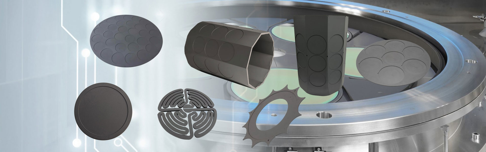
Semicorex katı CVD SiC halkaları, esas olarak gelişmiş yarı iletken endüstrisindeki plazma dağlama ekipmanının reaksiyon odalarında kullanılan yüksek performanslı halka şeklindeki bileşenlerdir. Semicorex katı CVD SiC halkaları, sıkı malzeme seçimi ve kalite kontrolünden geçirilerek benzersiz malzeme saflığı, olağanüstü plazma korozyon direnci ve tutarlı operasyonel performans sunar.
Devamını okuTalep Gönder
Silisyum Karbür Odak Halkaları
Önemli halka parçaları olan silisyum karbür odak halkaları, yarı iletken plazma aşındırmada levha aşındırma işleminin tek biçimliliğini ve stabilitesini geliştirmek için özel olarak tasarlanmıştır. Düzgün plazma dağıtımını teşvik etme ve elektrik alanı ortamını optimize etme konusundaki mükemmel performanslarıyla ünlüdürler.
Devamını okuTalep Gönder
CVD SiC Duş başlıkları
Semicorex CVD SiC Duş Başlıkları, gelişmiş yarı iletken üretiminde CCP ve ICP gravür sistemleri için tasarlanmış yüksek saflıkta, hassas mühendislikle tasarlanmış bileşenlerdir. Semicorex'i seçmek, en zorlu plazma işlemleri için üstün malzeme saflığı, işleme doğruluğu ve dayanıklılık ile güvenilir çözümler elde etmek anlamına gelir.*
Devamını okuTalep Gönder
Kenar halkaları
Semicorex kenar halkaları dünya çapında önde gelen yarı iletken Fabs ve OEM'ler tarafından güvenilir. Sıkı kalite kontrolü, gelişmiş üretim süreçleri ve uygulama odaklı tasarımla Semicorex, takım ömrünü uzatan, gofret tekdüzeliğini optimize eden ve gelişmiş işlem düğümlerini destekleyen çözümler sunar.*
Devamını okuTalep Gönder
Gaz dağıtım plakaları
CVD SIC'den yapılmış Semicorex Gaz Dağıtım Plakaları, plazma aşındırma sistemlerinde, gofret boyunca düzgün gaz dispersiyonu ve tutarlı plazma performansı sağlamak için tasarlanmış kritik bir bileşendir. Semicorex, eşsiz malzeme saflığı, mühendislik hassasiyeti ve ileri yarı iletken üretim taleplerine göre uyarlanmış güvenilir destek sunan yüksek performanslı seramik çözümler için güvenilir bir seçimdir.*
Devamını okuTalep Gönder
Katı SiC Duş Başlığı
Katı SiC Duş Başlığı, özellikle kimyasal buhar biriktirme (CVD) işlemleri için tasarlanmış, yarı iletken üretiminde önemli bir bileşendir. Gelişmiş malzeme teknolojisinde lider olan Semicorex, öncü gazların alt tabaka yüzeyleri üzerinde üstün dağılımını sağlayan Katı SiC Duş Başlıkları sunmaktadır. Bu hassasiyet, yüksek kaliteli ve tutarlı işleme sonuçları elde etmek için hayati öneme sahiptir.**
Devamını okuTalep Gönder
Semicorex uzun yıllardır CVD sic üretmektedir ve Çin'deki profesyonel CVD sic üreticilerinden ve Tedarikçilerinden biridir. Toplu paketleme sağlayan gelişmiş ve dayanıklı ürünlerimizi satın aldıktan sonra, hızlı teslimatta büyük miktarı garanti ediyoruz. Yıllar boyunca, müşterilere özelleştirilmiş hizmet sağladık. Müşterilerimiz ürünlerimizden ve mükemmel hizmetimizden memnun. Güvenilir uzun vadeli iş ortağınız olmayı içtenlikle bekliyoruz! Fabrikamızdan ürün almaya hoş geldiniz.